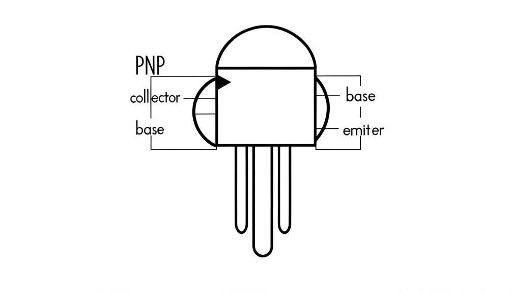
How to Identify and Draw the Circuit Symbol for a Transistor
The circuit symbol for a transistor depends on its type. For Bipolar Junction Transistors (BJTs), an NPN transistor symbol features an arrow pointing outward from the emitter, while a PNP transistor has an arrow pointing inward.
Both symbols comprise three terminals: collector, base, and emitter. Proper orientation and terminal identification are essential for accurate circuit functionality.
Field-Effect Transistors (FETs), like JFETs and MOSFETs, have distinct symbols indicating N-channel or P-channel types. These symbols are fundamental in designing and analyzing electronic circuits effectively.
Gaining a thorough understanding of these symbols will enhance circuit performance and reliability.

Key Takeaways
- The NPN transistor symbol features an arrow pointing outward from the emitter.
- The PNP transistor symbol has an arrow pointing inward towards the emitter.
- Transistor symbols consist of three terminals: collector, base, and emitter.
- Symbols vary based on transistor types such as NPN, PNP, N-channel, and P-channel.
- Correct interpretation of transistor symbols ensures proper circuit functionality and design.
Types of Transistors
Transistors, pivotal components in modern electronics, are primarily categorized into Bipolar Junction Transistors (BJTs) and Field-Effect Transistors (FETs), each with distinct operating principles and applications.
BJTs operate based on the injection and control of charge carriers across a junction, encompassing NPN and PNP types. They are known for their high gain and are widely used in amplification and switching applications.
FETs, including Junction FETs (JFETs) and Metal-Oxide-Semiconductor FETs (MOSFETs), function via an electric field influencing the conductivity of a semiconductor channel. FETs are valued for their high input impedance and are prevalent in digital circuits, signal modulation, and analog switches.
Understanding these types aids in selecting the appropriate transistor for specific electronic functions.
NPN Transistor Symbol
The NPN transistor symbol is distinguished by its specific orientation, where the arrow on the emitter leg points outward, indicating the direction of conventional current flow from the collector to the emitter.
This orientation is essential for understanding the biasing and operational characteristics of the transistor in various circuits. The symbol's design facilitates the identification of the three terminals: the collector, base, and emitter, which are necessary for accurate circuit design and analysis.
Symbol Orientation Explained
Understanding the orientation of an NPN transistor symbol is vital for accurately interpreting circuit diagrams and guaranteeing proper functionality in electronic designs. The NPN transistor symbol consists of three terminals: the emitter, base, and collector.
The emitter is denoted by an arrow pointing outward, indicating conventional current flow. The base is situated at the center, acting as the control terminal. The collector is opposite the emitter, receiving the current controlled by the base-emitter junction.
Correctly identifying these terminals is essential for circuit assembly and troubleshooting. Misorientation can lead to improper biasing, resulting in circuit malfunction or damage.
Precise attention to the symbol's orientation guarantees the designed circuit operates as intended, maintaining reliability and performance.
Current Flow Direction
Accurately interpreting the current flow direction in an NPN transistor symbol is fundamental for guaranteeing the correct operation of electronic circuits. The NPN transistor allows current to flow from the collector to the emitter when a sufficient base current is applied. This flow direction is essential for effective circuit design and troubleshooting.
- Collector to Emitter Current (I_C): This primary current flows from the collector to the emitter and is controlled by the base current.
- Base Current (I_B): A smaller current entering the base terminal, which regulates the larger collector-emitter current.
- Conventional Current Flow: Utilizes the arrow on the emitter, indicating current flows out of the emitter in an NPN transistor, reinforcing the collector-to-emitter direction.
Understanding these elements guarantees precise circuit functionality.
PNP Transistor Symbol

In a PNP transistor symbol, the arrow on the emitter terminal points inward toward the base, indicating the direction of conventional current flow when the device is in active mode.
This inward-pointing arrow is an essential characteristic distinguishing PNP transistors from their NPN counterparts. The PNP transistor consists of a layer of N-type semiconductor material sandwiched between two P-type layers.
When a small current flows out of the base, it allows a larger current to flow from the emitter to the collector. The symbol is pivotal for correctly identifying the transistor's orientation and ensuring proper circuit functionality.
Understanding this symbol allows engineers to appropriately design and troubleshoot circuits involving PNP transistors.
Reading Transistor Symbols
To accurately interpret transistor symbols, one must be familiar with the various graphical representations of each transistor type and the specific designations for their terminals. Transistors, whether Bipolar Junction Transistors (BJTs) or Field-Effect Transistors (FETs), have distinctive symbols that indicate their type and function. Each symbol includes specific annotations for the three primary terminals: the emitter, base, and collector for BJTs, and the source, gate, and drain for FETs.
Key points to note include:
- Arrow Direction: Indicates the type of transistor (NPN or PNP for BJTs, and N-channel or P-channel for FETs).
- Terminal Positioning: Proper identification of terminals is essential for accurate circuit interpretation.
- Symbol Variations: Different standards may present slight variations in symbols, requiring careful attention.
Understanding these elements is vital for accurate circuit analysis.
Applications in Circuits

Transistors play a pivotal role in circuits by enabling amplification and switching functionalities. They act as key components in increasing signal strength and controlling current flow.
They are also integral to signal modulation techniques, facilitating the encoding of information onto carrier signals through amplitude, frequency, or phase modulation.
These applications underscore the versatility and indispensability of transistors in modern electronic systems.
Amplification and Switching Uses
Leveraging their unique ability to control current flow, transistors serve pivotal roles in both amplification and switching applications within electronic circuits. In amplification, they boost weak signals to higher levels, essential in audio and radio frequency circuits.
As switches, transistors can turn current on and off rapidly, vital for digital logic circuits and power regulation.
Key applications include:
- Audio Amplifiers: Enhancing sound signals in devices like radios and musical instruments.
- Digital Logic Circuits: Forming the building blocks of microprocessors and memory storage.
- Switching Power Supplies: Efficiently converting and regulating power in electronic devices.
Through these applications, transistors enable complex functionalities and high performance in modern electronic systems.
Signal Modulation Techniques
Signal modulation techniques, essential for encoding information onto carrier signals, play a critical role in optimizing the performance and efficiency of electronic communication systems. Various methods such as Amplitude Modulation (AM), Frequency Modulation (FM), and Phase Modulation (PM) are employed to achieve effective signal transmission.
In transistor-based circuits, these modulation techniques can be implemented through proper biasing and configuration of transistor parameters. For instance, a transistor in a common-emitter configuration can be utilized for amplitude modulation by varying the base current. Similarly, frequency modulation can be achieved by integrating reactive components with transistors.
These modulation techniques ensure robust communication by improving signal integrity and reducing susceptibility to noise, thereby facilitating reliable data transfer in complex electronic systems.
Common Mistakes
One prevalent error in interpreting transistor circuit symbols is the confusion between the emitter and collector terminals, which can greatly impact circuit functionality. This mistake can lead to improper current flow, resulting in circuit failure or inefficiency.
Common mistakes include:
- Incorrect Terminal Identification: Misidentifying the emitter and collector can cause the transistor to operate incorrectly, as these terminals are not interchangeable.
- Improper Biasing: Applying incorrect bias voltages due to terminal confusion can disrupt the transistor's active region operation, leading to signal distortion or amplification failure.
- Symbol Misinterpretation: Failing to distinguish between NPN and PNP transistor symbols can result in inverted current flow, thereby compromising the circuit's intended design and performance.
Understanding these common errors is essential for optimizing transistor-based circuit designs.
Conclusion
Transistor symbols serve as the cartographic map guiding engineers through the intricate landscape of electronic circuits. Understanding these symbols, from NPN to PNP, is essential for accurate circuit design and functionality.
Just as a single misread map legend can lead a traveler astray, misinterpreting transistor symbols can result in circuit failures and inefficiencies. Mastery over these symbols enables the creation of robust and efficient electronic systems, underscoring their critical role in modern technology.


